Solid-State Drive Introduction
Introduction to Solid-State Drive (SSD) for Beginners.
This article serves as a beginner’s guide to the SSD and SSD controllers. A significant portion of the content is carefully selected from various sources on the internet, as I’m relatively new to this field. Nonetheless, the article includes thorough discussions and emphasizes key points to offer an enhanced learning path for newcomers.
Learning Resources
- SNIA contains a lot of white papers and educational materials.
- Coding for SSDs from Emmanuel Goossaert. Very thorough in-depth introductions.
- Modern SSD Design, course from ETZ Zurich. It has rich contents with lecture slides and videos.
Basic Introduction
Often the terms “Flash Storage” and “SSD” are used interchangeably, but while these technologies both store data, it’s worth knowing some key differences between the two.
As described in this blog
To put it plainly, most SSDs will use flash memory, but not all flash memory devices are considered SSDs.
Performance
For example, while Client SSD use cases may largely be concerned with average response times, the Enterprise use cases are often more interested in maximum response times and the frequency and distribution of those response times.
SSD Controller
The SSD (Solid State Drive) controller serves as a critical component in managing the operations of an SSD. It plays a pivotal role in ensuring the efficient and reliable functioning of the SSD.
- Interface Management:
The SSD controller manages the communication interface between the SSD and the host system. It ensures proper interaction through interfaces like SATA, PCIe (NVMe or AHCI), or other storage protocols.
- Command Processing:
The controller interprets and processes commands received from the host system. It executes read and write operations, manages data transfers, and handles other storage-related commands.
- Flash Translation Layer (FTL):
The FTL is a crucial component of the SSD controller. It performs the mapping between logical block addresses (used by the host system) and physical locations on the NAND flash memory. This includes wear leveling to distribute write and erase cycles evenly across the memory cells.
- Wear Leveling:
Wear leveling is a key function that extends the lifespan of the SSD by ensuring that write and erase cycles are distributed evenly across the NAND flash memory. The controller manages this process to prevent premature wear on specific memory cells.
- Error Correction:
The controller implements error correction algorithms to address bit errors that may occur during read and write operations. This enhances data integrity and reliability.
Bad Block Management:
Bad blocks may develop over time in NAND flash memory. The SSD controller identifies and manages these bad blocks, ensuring that data is stored in reliable locations and minimizing the impact of defective memory cells.
- Garbage Collection:
Garbage collection is the process of reclaiming space by erasing blocks that are no longer in use. The SSD controller manages this process to optimize storage space and maintain overall performance.
- Power Management:
The controller may incorporate power management features, such as transitioning the SSD between different power states (active, idle, sleep) to optimize power consumption and extend battery life in mobile devices. Firmware Execution:
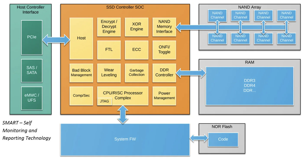 Figure from SemiconductorEngineer
Lifecycle
Each cell has a maximum number of P/E cycles (Program/Erase), after which the cell is considered defective. NAND-flash memory wears off and has a limited lifespan.
Please refer to How Controllers Maximize SSD Life for details about how a controller could prolong the SSD lifespan through the following methods.
- Wear Leveling
- External Data Buffering
- Improved ECC
- Other Error Management
- Reduced Write Amplification
- Over Provisioning
- Feedback on Block Wear
- Internal NAND Management
Parallelism
Parallelism distinguishes NVMe from the conventional SATA interface. Traditional hard disk drives (HDDs) lack support for true parallelism in read and write operations, especially compared to modern NAND-based SSDs. While SATA continues to be prevalent, the landscape shifts with the emergence of SSD technology. HDDs, relying on SATA, face limitations in achieving true parallelism. With SSDs gaining prominence, NVMe is poised to take a more central role soon as a protocol optimized for SSD’s inherent features of parallelism.
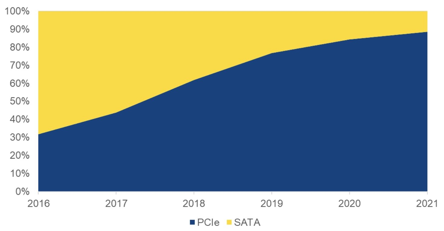 Source: Intel Forecasting, Q2’18
The following parallel introduction is from Coding for SSDs.
- Channel-level parallelism. The flash controller communicates with the flash packages through multiple channels. Those channels can be accessed independently and simultaneously. Each individual channel is shared by multiple packages.
- Package-level parallelism. The packages on a channel can be accessed independently. Interleaving can be used to run commands simultaneously on the packages shared by the same channel.
- Chip-level parallelism. A package contains two or more chips, which can be accessed independently in parallel. Note: chips are also called “dies”.
- Plane-level parallelism. A chip contains two or more planes. The same operation (read, write or erase) can be run simultaneously on multiple planes inside a chip. Planes contain blocks, which themselves contains pages. The plane also contains registers (small RAM buffers), which are used for plane-level operations.
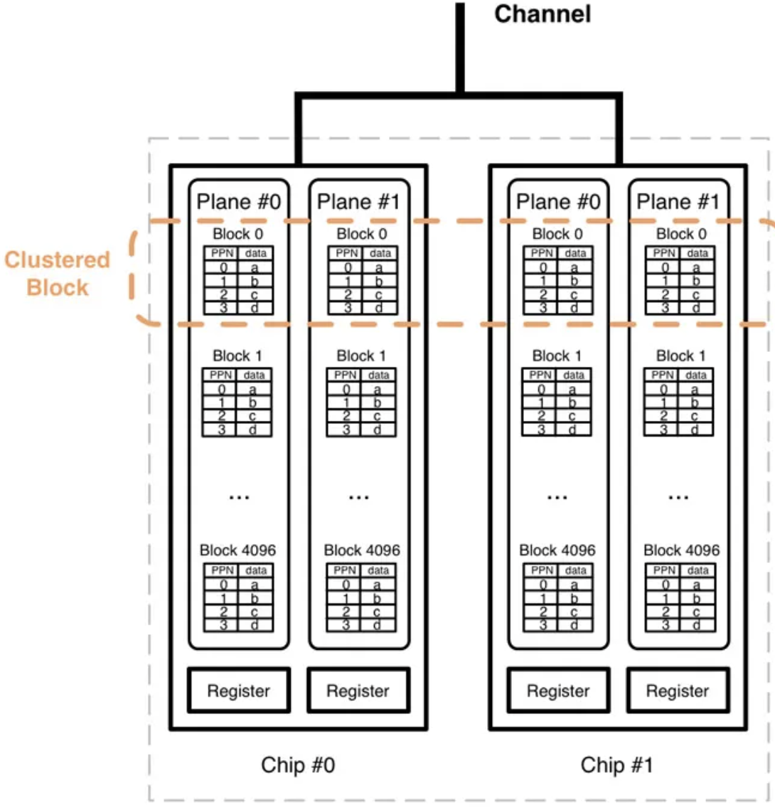 NAND Flash Package
Further Reading
- An example of Tailor-Made Enterprise SSDs from SwissBit.
- A README SSD guide includes basic introduction of SSD and many other related knowledge.
- MQSim: A Simulator for Modern NVMe and SATA SSDs
- The Open-Channel SSD User Space Library
- SSD Guy
Leave a comment